Contents:
カーボンナノチューブ(Carbon nanotube)
単層カーボンナノチューブ(SWCNT: single-walled carbon nanotube)とは、 炭素原子によって構成されるナノ物質であり、名前の通りナノサイズのチューブである。
CNTの先端構造
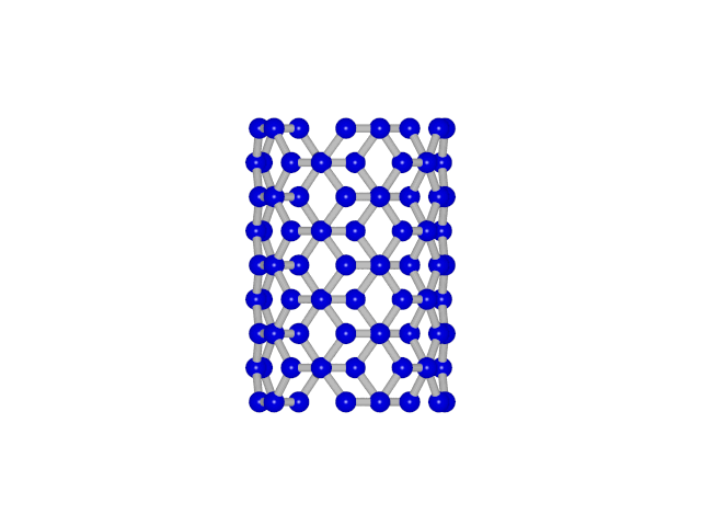
カーボンナノチューブ先端の電子雲を観察した研究についてご紹介致します。グラフェンシートは、炭素原子6個でできた六員環でできています。

そのグラフェンシートを丸めた構造をしているのが、カーボンナノチューブです。

カーボンナノチューブを合成する場合、金属触媒という物に炭素を供給することで、 カーボンナノチューブが成長します!こんな感じです!

カーボンナノチューブの先端には、キャンプというものがあり、 合成する際に、初めに、金属触媒にキャップ構造ができ、その後、チューブ本体が伸びます! キャップには、炭素原子5個でできた五員環が入っています。

この五員環の部分が、とがっています! 次の画像の青色の部分!

そのとんがった部分の電子雲を実験で観察することができます! それが、私の博士号の研究の1つです。
直径などを計測した単層カーボンナノチューブ先端の電子雲を観察しました。 ぼんやりした映像が、単層カーボンナノチューブ先端の電子雲です! また、動画の33 秒から35秒の間に、水素原子が吸着したことが観察できています。
これらの研究成果は、次の論文にまとめています。
Surf. Interface Anal. DOI: 10.1002/sia.5611 (2014)
以下、編集中です。
SWCNT tip1,2
A single-walled carbon nanotube (SWCNT) with well-defined structure has a potential as a probe of scanning microscopy. However, SWCNT tip has not been applied to practical use yet because of the difficulty in the tip preparation. We have developed a technology for fabrication of SWCNT tips with the yield rate of 25%.
SEM images showing typical types of SWCNT tips and their abundance.
(a) Off-axis growth, 30%;
(b) long on-axis growth, 10%; and
(c) short on-axis growth, 3%.2
STM application1
Various lengths and shapes of SWCNT tips were examined as the probe of ultrahigh vacuum scanning tunneling microscopy (STM). We found that the length of SWCNT was a crucial factor for the application to STM. Atomic-scale resolution could be obtained on the surface of highly oriented pyrolytic graphite with an SWCNT tip shorter than 300 nm. In the case of ring type SWCNT tip, which used the side wall of SWCNT, the STM images depended on the scan direction due to the half-ring shape, and atomic-scale resolution could be obtained when scanned along the circumference direction of the ring. Although the stability of the SWCNT tip during scanning needs to be improved, present results prove the potential of SWCNT for STM probes.
STM observation results with a straight type SWCNT tip.
(a) SEM image of an SWCNT tip.
(b) STM image of HOPG with the SWCNT tip.
1
FEM application2
Field electron emission (FE) from a structure-defined single-walled carbon nanotube (SWCNT) was observed experimentally. FE image from an individual diameter-defined SWCNT could be observed. The diameter of SWCNT was ~ 1.73 nm, and the FE current of 2.2 × 10⁻⁷ A was obtained at a low applied voltage of 270 V.
FEM observation results of the SWCNT tip in 1.3 × 10⁻⁷ Pa.
(a) Snapshots of the FEM image.
(b) Time variation of I (solid line) and V (dashed line).
2
References
1 e-J. Surf. Sci. Nanotech. 11, 105-108 (2013)2 Surf. Interface Anal. DOI: 10.1002/sia.5611 (2014)